GPIO Pin Functionality in FL2G and Ladybug3
Download PDF - New_GPIO_Functionality_In_FL2G
Overview
With the introduction of the Flea2 FL2G-13S2M/C, FL2G-50S5M/C and Ladybug3 20S4C models, the GPIO functionality has been enhanced to provide one opto-isolated input pin and one opto-isolated output pin. The opto-isolators provide protection against voltage spikes or ground loop conditions that may otherwise cause damage to the camera. It is also designed to meet industrial application requirements for +5 V to +24 V triggering and strobe, and minimize the need for external current limiting resistors.
|
|
Customers requiring four output lines (e.g. for sending a strobe pulse off each pin) will be directly affected by this change due to the presence of only 3 possible output lines (one opto-isolated, two bi-directional). |

FL2G and FL2 GPIO Comparison
The following section details the similarities and differences in GPIO functionality between the new FL2G and original FL2 models.
|
|
All Flea2 FL2 and FL2G models use the same Hirose HR25-7TR-8SA female GPIO connector. |

Figure 1: Hirose 8-pin connector used on FL2 and FL2G
|
Spec |
FL2 |
FL2G |
|
GPIO0 (Pin 1) |
Bi-directional input/output |
Opto-isolated input |
|
GPIO1 (Pin 2) |
Bi-directional input/output |
Opto-isolated open collector output |
|
GPIO2 (Pin 3) |
Bi-directional input/output |
|
|
GPIO3 (Pin 4) |
Bi-directional input/output |
|
|
GND |
Ground pin for all pins |
Ground pin for bi-directional IO, Vext, +3.3 V |
|
GND |
Ground pin for all pins |
Ground pin for opto-isolated IO pins |
|
Vext |
Power camera externally |
|
|
+3.3V (Pin 8) |
Power external devices |
|
GPIO0 (Opto-Isolated Input) Circuit
The figure below shows the schematic for the opto-isolated input circuit.

Figure 2: Optical input circuit
- Logical 0 input voltage: 0 VDC to +1 VDC (voltage at OPTO_IN)
- Logical 1 input voltage: +1.5 VDC to +30 VDC (voltage at OPTO_IN)
- Maximum input current: 8.3 mA
- Behavior between 1 VDC and 1.5 VDC is undefined and input voltages between those values should be avoided
- Input delay time: 4 μs
GPIO1 (Opto-Isolated Output) Circuit
The figure below shows the schematic for the opto-isolated output circuit. The maximum current allowed through the opto-isolated output circuit is 25mA (limit by PTC resistor), and the output impedance is 140Ω.

Figure 3: Optical output circuit
Response Time
The following table lists the switching times for the opto-isolator in the output pin, assuming an output VCC of 5 V and a 1 kΩ resistor.
|
Parameter |
Value |
|
Delay Time |
9 μs |
|
Rise Time |
16.8 μs |
|
Storage Time |
0.52 μs |
|
Fall Time |
2.92 μs |
Sample Voltage / Resistor Combinations
The following table lists several external voltage and resistor combinations that have been tested to work with the opto-isolated output.
|
External Voltage |
External Resistor |
OPTO_OUT Voltage |
OPTO_OUT Current |
|
3.3 V |
1 kΩ |
0.56 V |
2.7 mA |
|
5 V |
1 kΩ |
0.84 V |
4.2 mA |
|
12 V |
2.4 kΩ |
0.91 V |
4.6 mA |
|
24 V |
4.7 kΩ |
1.07 V |
5.1 mA |
|
30 V |
4.7 kΩ |
1.51 V |
13.3 mA |
GPIO2 / 3 (Bi-Directional) Circuit

Figure 4: GPIO2 / 3 Circuit
Input Side
- Logical 0 input voltage: 0 VDC to +0.5 VDC (voltage at GPIO2 / 3)
- Logical 1 input voltage: +1.5 VDC to +30 VDC (voltage at GPIO2 / 3)
- Behavior between 0.5 VDC and 1.5 VDC is undefined and input voltages between those values should be avoided
|
|
To avoid damage, connect the ground (GND) pin first before applying voltage to the GPIO line. |

Output Side
The maximum output current allowed through the bi-directional circuit is 25mA (limit by PTC resistor), and the output impedance is 40Ω.
The following table lists several external voltage and resistor combinations that have been tested to work with the bi-directional GPIO when configured as output.
|
External Voltage |
External Resistor |
GPIO2/3 Voltage |
|
3.3 V |
1 kΩ |
0.157 V |
|
5 V |
1 kΩ |
0.218 V |
|
12 V |
1 kΩ |
0.46 V |
|
24 V |
1 kΩ |
0.86 V |
|
30 V |
1 kΩ |
0.966 V |
The following table lists the switching times for a standard GPIO pin, assuming an output VCC of 5V and a 1kΩ resistor.
|
Parameter |
Value |
|
Delay Time |
0.28 μs |
|
Rise Time |
0.06 μs |
|
Storage Time |
0.03 μs |
|
Fall Time |
0.016 μs |
Related Articles
-
 Application Story
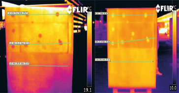
FLIR cameras support analysis and diagnosis of external thermal insulation systems
Read the Story -
 Case Study
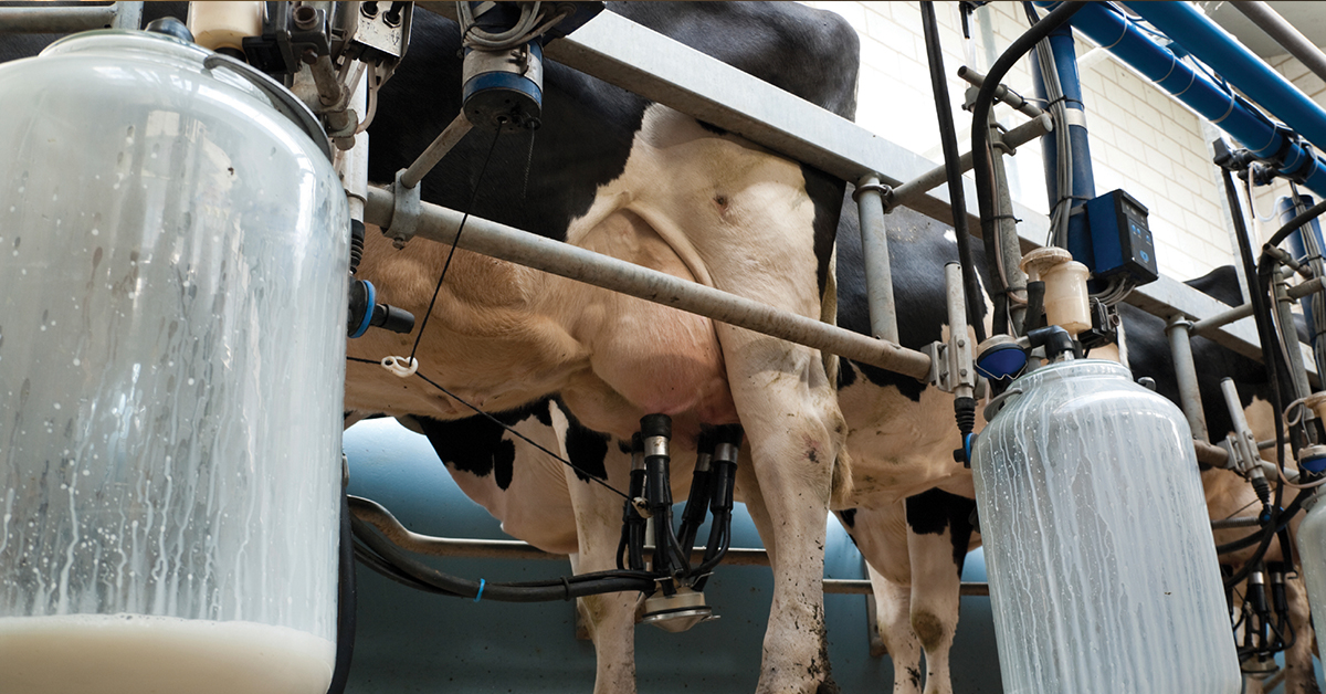
Automatic Health Check in Dairy Farms Using FLIR Thermal Imaging Cameras
Read the Story -
 Deep Learning
Comparing Deep Learning Cameras with Smart Cameras
Read the Story